

and it had a nice surprise inside !
Plug in under the disk drive, remove the CPU and plug in the board..... A Very Clean Design ! KUDOS !
Fun Facts- see below
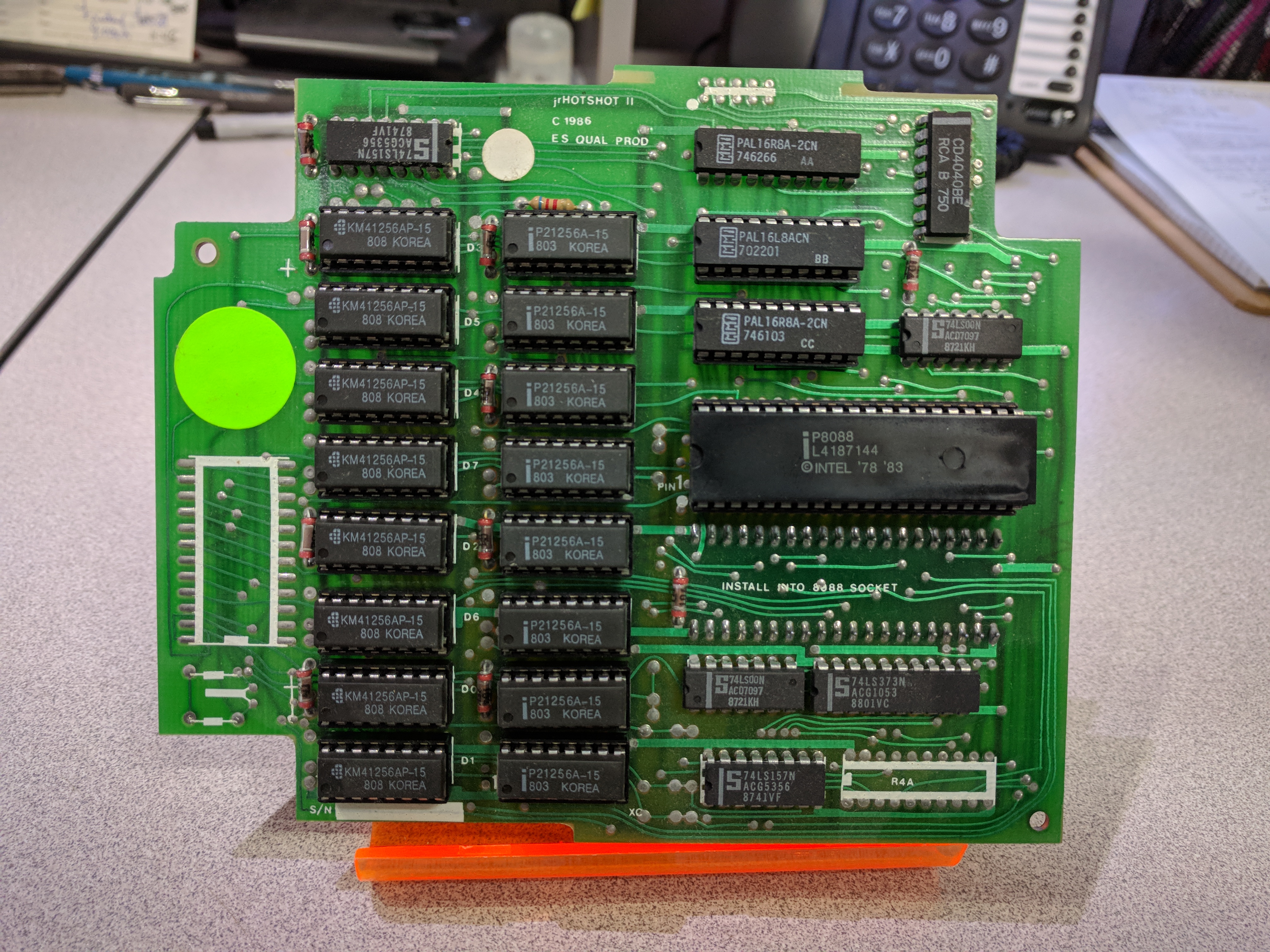
HOTSHOT II 640K ( Inventor Ed Strauss)
FUN FACTS
Looking closely at the HOT SHOT PCB, you will notice the traces on the board are curved across the board.
Why ? Back in the early 80s', laying put a PCB was done on a Light Table usually 2X or better the True size of the board.
Each trace was put down with different size rolls of mylar black tape, Power and Ground traces were typically the larger size.
All tape would be run from point to point by hand, and the curves were easy to do with the tape as you pressed it onto the large
sheet of mylar. The Holes were precut and ready to place down, beneath the mylar sheet was a grid (sometime) on mylar that
the layout person could use to keep the tape and press down holes in line.
The tape was easier to lay in a continuous run from one pin to the other and with gentle curves to go around components as needed.
Early boards were usually 2 layer and had Power and Ground traces, usually wider to carry the current, on both Top and Bottom layers.
This method was done by some talented folks, and with precision.
You can imagine the board checking for accuracy that had to be done to ensure all tape was properly put down to match the schematic.
So when you look at these old boards, smile and have a little appreciation for the time it took to get these boards from hand drawn schematics
to mylar taped PCB layout to the final copper bare board ready for components.
Yes I did this back in the day, but much more enjoy the advantages of the high end layout software of Altium.

